Intel's Advancements in EMIB and Foveros Packaging Technologies: What's Next?
| Shelf | AI & ML |
|---|---|
| Date in | |
| Readers | 440 |
Intel's EMIB and Foveros technologies are evolving to address increasing demands for AI and HPC. This article explores their advancements, roadmaps, and practical implications.
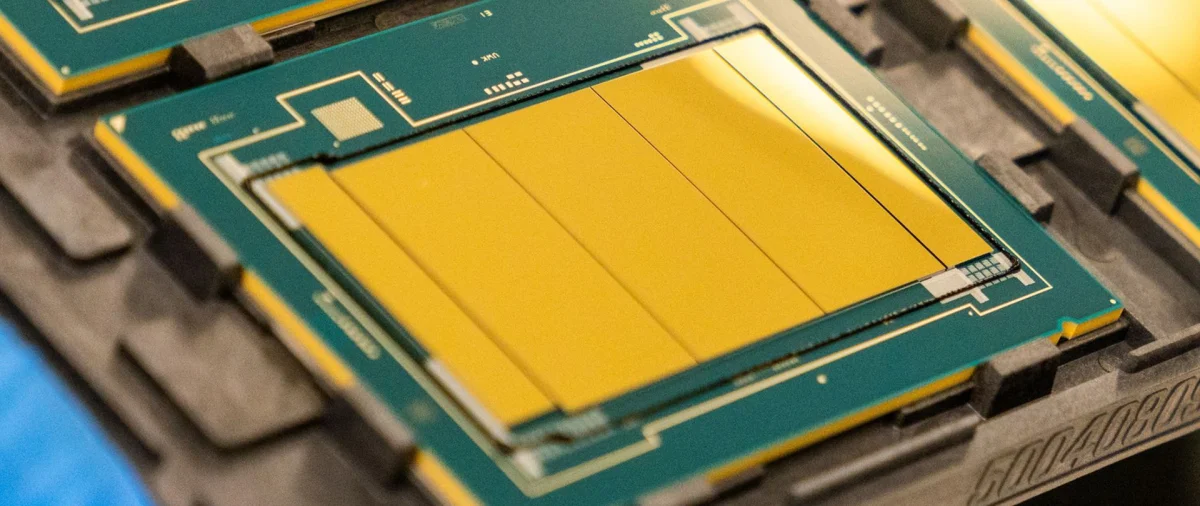
Advanced packaging technologies have become critical for the design of high-performance CPUs and GPUs, particularly with Intel's Embedded Multi-die Interconnect Bridge (EMIB) and Foveros methods being employed in virtually all of the company's high-end client and data center processors. This evolution raises questions about the future directions of these technologies, especially given their significant role in enhancing performance and cost efficiency. Here, we’ll take an in-depth look at the current state of EMIB and Foveros, their development roadmaps, and their implications for the semiconductor industry.
The Rise of EMIB and Foveros
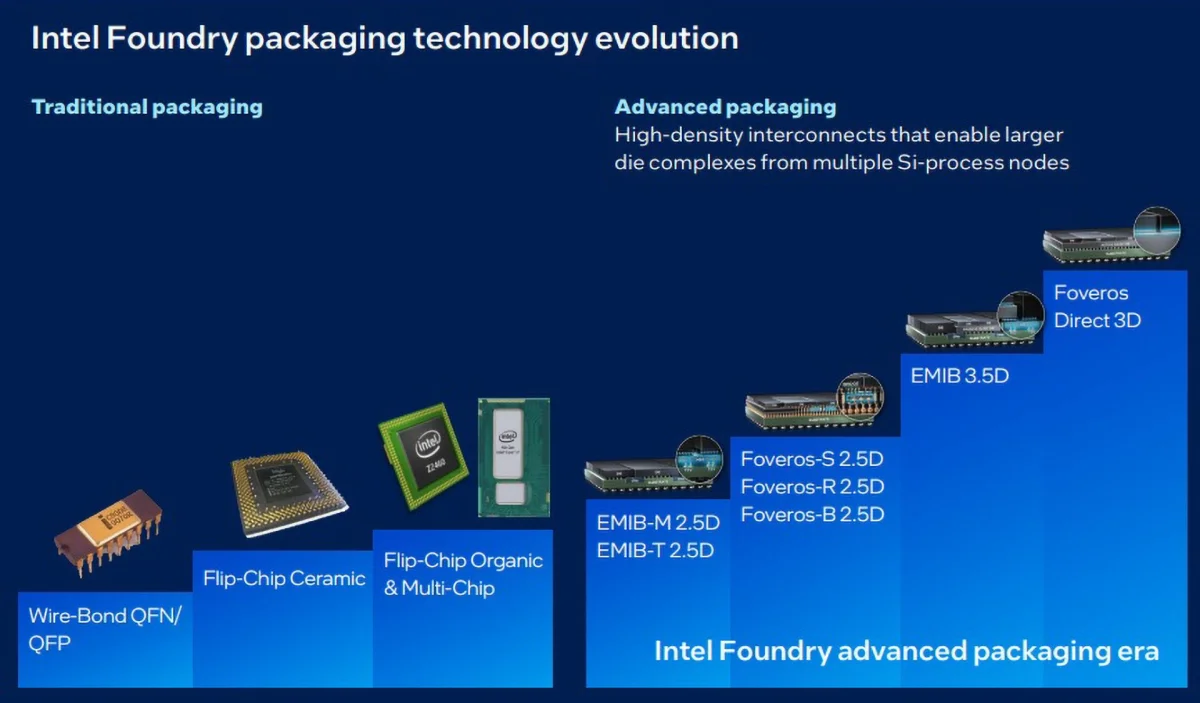
Intel initiated its journey into advanced packaging back in 2017 with chips like the Kaby Lake-G CPUs and Stratix 10 FPGAs. Although these technologies initially didn't attract much attention, both Intel and its competitors have since recognized the value of advanced packaging in meeting the demands of modern computing. Intel laid out its roadmap for multi-chiplet processors that utilize both EMIB and Foveros in 2020, especially after encountering challenges with its 10nm process technology. The multi-chiplet strategy proves to be an efficient way to enhance performance while managing manufacturing costs efficiently.
Over the years, Intel has transitioned from using separate packaging technologies to integrating EMIB and Foveros. These methods are increasingly complementary, potentially leading to the creation of large system-in-packages (SiPs) that combine both technologies. While Intel aims to produce SiPs that can grow substantially in size using EMIB and Foveros Direct 3D, there’s still a journey ahead to reach those ambitious targets.
EMIB: Transformation and Innovations
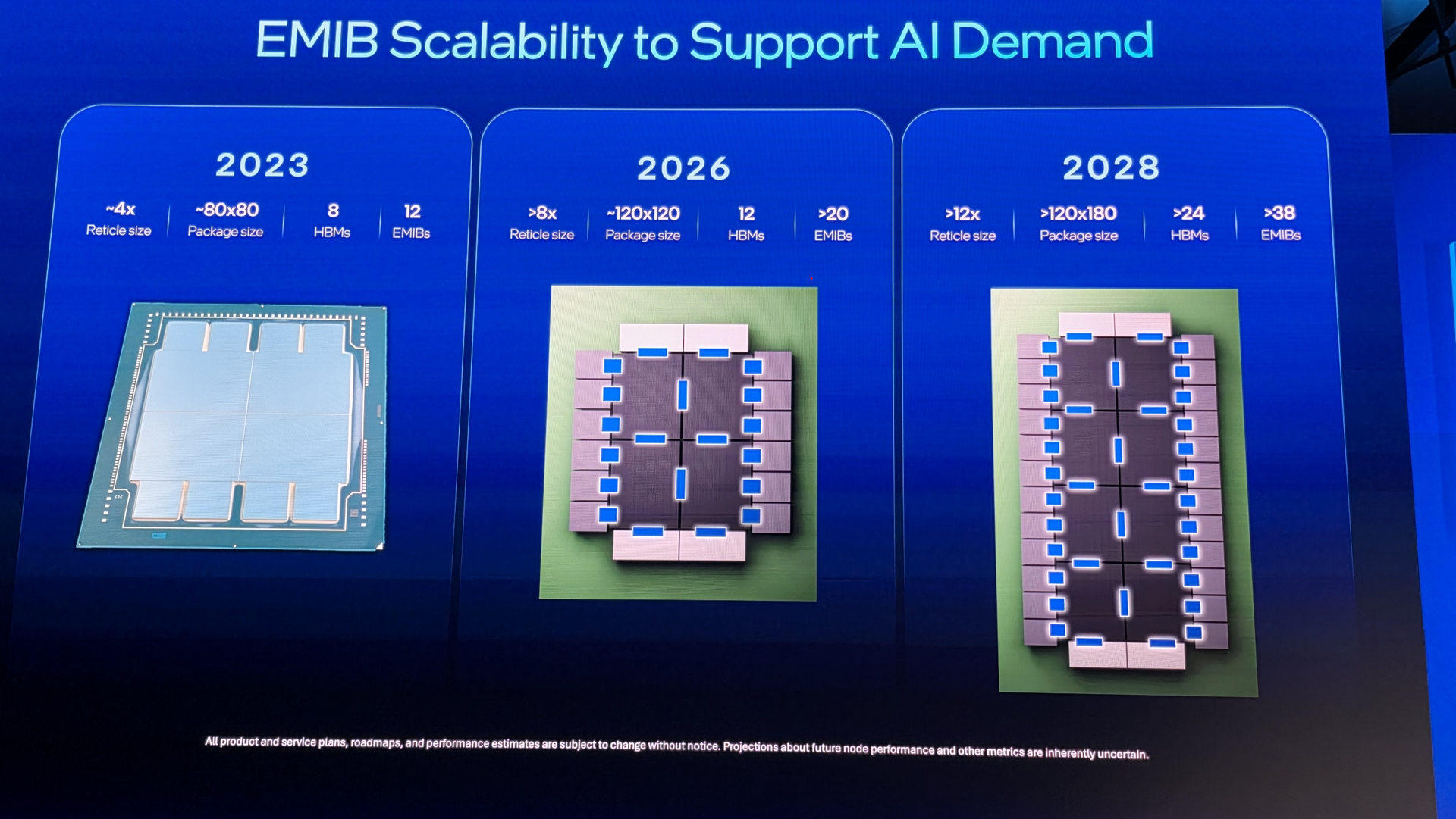
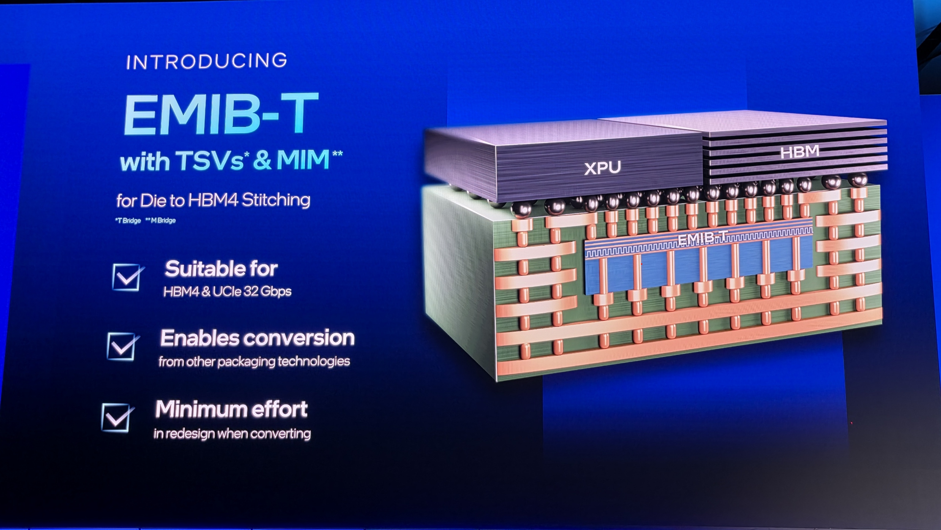
EMIB has evolved significantly since it commenced high-volume manufacturing, going from a relatively simple means of connecting adjacent chiplets to a sophisticated technology that underpins Intel's higher-end data center processors. Future iterations of EMIB are set to accommodate multi-kilowatt SiPs, enhancing the capabilities of AI accelerators and other high-performance applications that rely on exceptional power delivery.
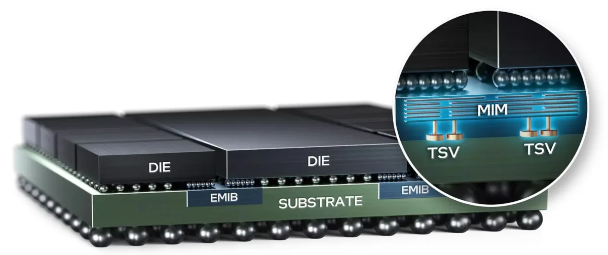
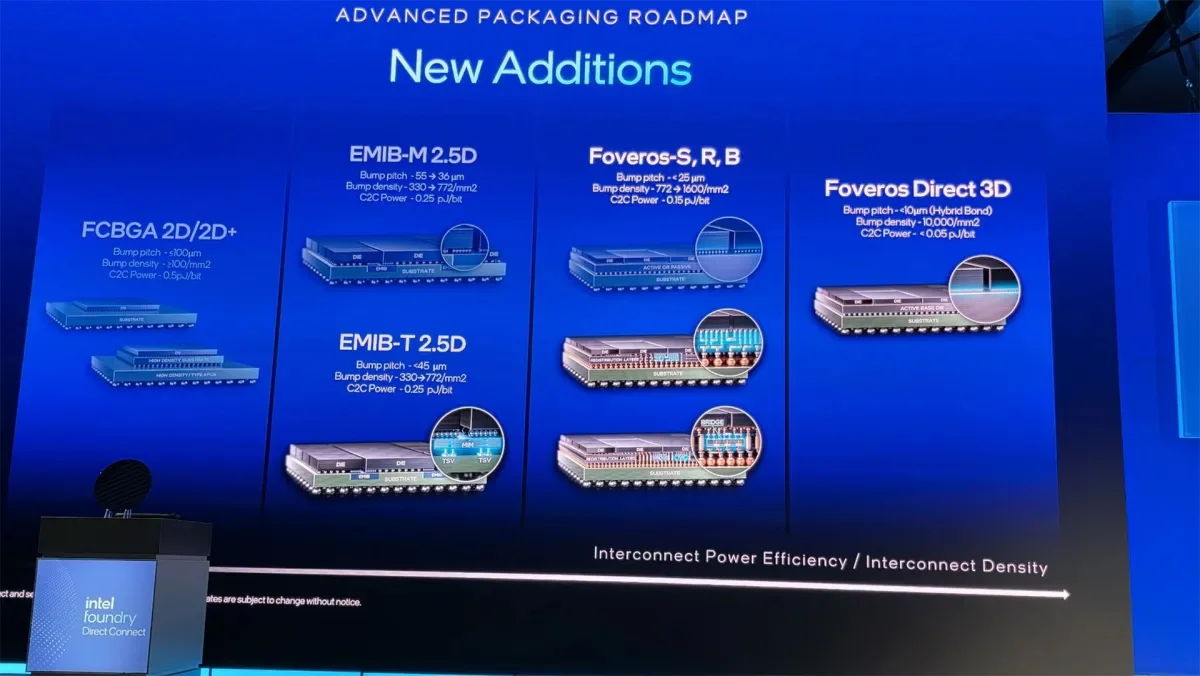
Intel has been refining the architecture of EMIB by implementing finer bump pitches that boost interconnect density. Initially set at 55 µm, the bump pitch has decreased to 45 µm, with plans to reduce it further to 36 µm and eventually to 25 µm. Such improvements will significantly enhance chiplet edge connectivity. More advanced versions of EMIB introduce innovations like EMIB-M, which integrates metal-insulator-metal (MIM) capacitors for better power integrity, and EMIB-T, which includes through-silicon vias (TSVs) that facilitate vertical power distribution. As power delivery becomes a crucial constraint, these enhancements improve current density and voltage stability significantly.
| 1st Gen | 2nd Gen | EMIB-M | EMIB-T | EMIB-T evo | EMIB-T glass | |
| Bump Pitch | 55 µm | 45 µm | 45 µm ~ 36 µm | 45 µm ~ 36 µm | 25 µm | |
| Number of Bridges | 6 | 12 | >20 | >38 | ? | ? |
| Bump Density | 330 mm² | 494 mm² | 494 => 772 mm² | 494 => 772 mm² | 1600 mm² | 1600 mm² |
| C2C Power | 0.5 pJ/bit | 0.3 - 0.5 pJ/bit | 0.25 pJ/bit | 0.25 pJ/bit | ? | ? |
| TSV | - | - | - | + | + | + |
| Die Complex | 2X reticles | 4X reticles | 8X reticles | 12X reticles | ? | panel |
| HBM Stacks | 4 | 8 | 12 | 24 | ? | ? |
| Capacitor | - | - | MIM | MIM | MIM (?) | MIM (?) |
| Substrate | organic | organic | organic | organic | organic | glass |
| Package size (mm) | 50 × 50 | 80 × 80 | 120 × 120 | 120 × 180 | ? | 240 × 240 (?) |
| Year | 2017 - 2023 | 2023 | 2024 - 2026 | 2028 | ? | 2030+ |
This transformation positions EMIB as a viable alternative to traditional silicon interposers, emphasizing its adaptability for AI-driven applications. Future plans indicate a shift toward integrating glass-core substrates to enhance performance and fabrication yields, addressing common issues related to warpage associated with organic materials.
Foveros: A Broadening Spectrum of Solutions
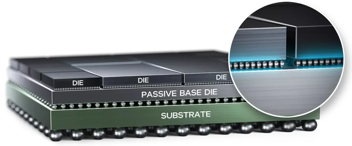
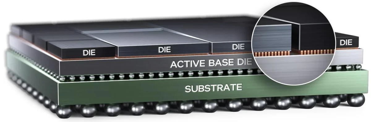
Foveros technology is evolving significantly beyond its initial chip-on-wafer model from 2019, which supported the Lakefield processor. Now, it represents a comprehensive family of 2.5D and 3D integration solutions that cater to a diverse array of applications, including high-performance computing (HPC) and artificial intelligence (AI) systems, alongside cost-effective client processors.
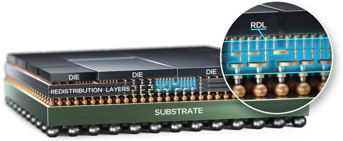
Originally built on an active silicon base, Foveros has diversified. The current Foveros family includes various implementations, such as Foveros-S, Foveros-R, and Foveros-B, which are aimed at different packaging needs. The latest evolution targets pitches under 25 µm, increased bump density from 772 to 1600 connections per mm², and reduces chip-to-chip interconnect power efficiency to an impressive 0.15 pJ/bit.
| Foveros-S | Foveros-R | Foveros-B | |
| Bump Pitch | 36µm => 25µm => | 36µm => 25µm => | 36µm => 25µm => |
| Hybrid Bonding | - | - | - |
| Local Bridges | - | - | Yes |
| Bump Density | 772-> 1600/mm² | 772-> 1600/mm² | 772-> 1600/mm² |
| C2C Power | 0.15 pJ/bit | 0.15 pJ/bit | 0.15 pJ/bit |
| TSV | - | - | ? |
| Die Complex | 4X reticle | RDL limited | Bridge limited |
| HBM Stacks | 8 (?) | Dependent upon interposer size | Dependent upon interposer size |
| Capacitor | - | ? | |
| Substrate | Organic | Organic | Organic |
| Package Size (mm) | ? | ? | ? |
| Year | 2019 | 2027 | ? |
Foveros-S stands out as the most advanced production-ready encapsulation in the family, facilitating integration on silicon interposers. Despite its current production constraints, the technology is poised for adaptations, including incrementally larger packages and denser interconnects that promise better performance.
Foveros-R represents an innovative design that eliminates the silicon interposer in favor of redistributed layers (RDL). By optimizing both cost and interconnect density while enabling heterogeneous integration among different chiplets, it's slated for production by 2027. This technology aims to further lower costs while enhancing connection efficiency through local active or passive bridges.
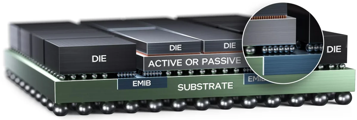
As for Foveros-B, it extends integrations to more complex structures, allowing for the combination of RDLs and local bridges that enhance connection density precisely where necessary. While some aspects of Foveros-B remain under wraps, there’s potential for it to leverage EMIB bridges and extend the advantages of MIM capacitors and integrated voltage regulators.
Foveros Direct 3D: Rethinking Vertical Stacking
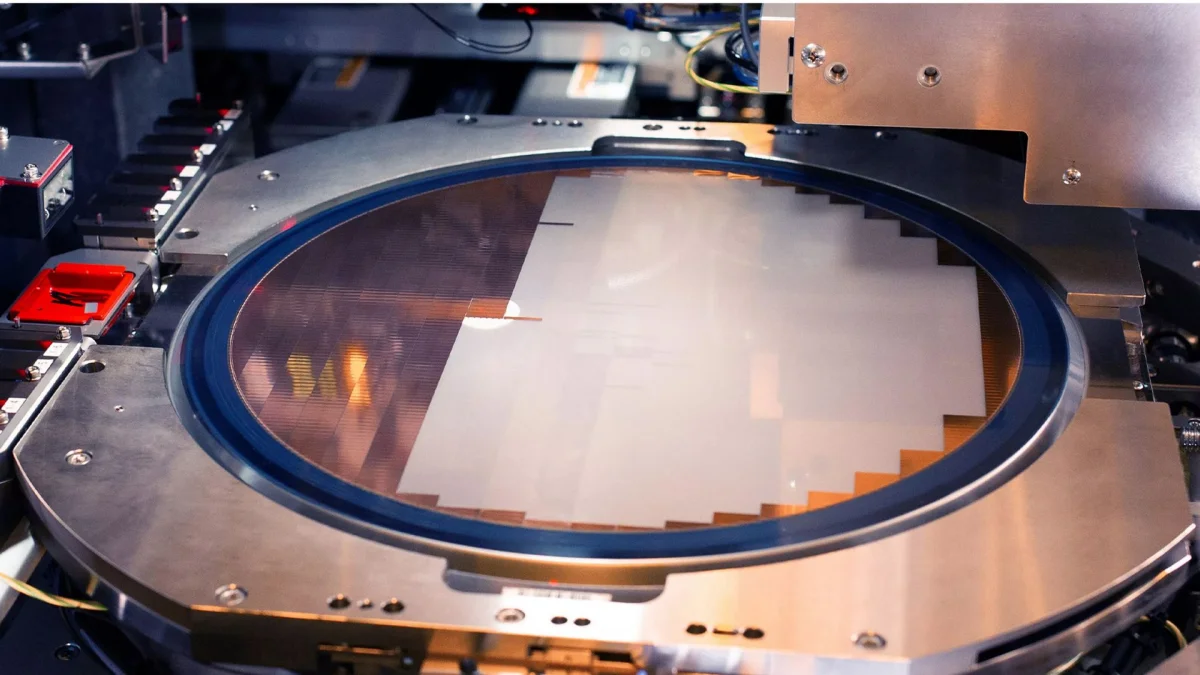
Foveros Direct 3D sets out to revolutionize the traditional notions of chip stacking by focusing on direct copper-to-copper bonding—bypassing the limitations of solder bumps. First deployed in 2026, this technique dramatically increases the interconnect density and diminishes electrical resistance while improving both thermal and power characteristics of the stacked dies.
Intel delineates its Foveros Direct 3D as capable of achieving bonding pitches below 10 µm—an unprecedented advancement compared to conventional microbump technologies. The initial generation supports a ~12,300/mm² pad density; the second generation aims for over 100,000/mm² pad density, significantly surpassing competitors. This illustrates not only enhanced power efficiency but also improved signal integrity, which is vital for high-performance CPUs and coprocessors in data-intensive applications.
| 1st Gen | 2nd Gen | |
| Joint | Cu–Cu hybrid bond (no solder) | Cu–Cu hybrid bond (no solder) |
| Pitch | 9 µm (public “sub-10 µm”) | 3 µm |
| Pad Density | ~12,300/mm² (Intel: >10,000) | Over 100,000/mm² |
| C2C Power | Not published (same class or lower) | |
| Base die | Active | Active |
| TSV | + (in base; 18A-PT adds pass-through TSV) | + |
| Capacitor/Extras in Base | MIM; Clearwater Forest adds LLC + IVR | MIM; Clearwater Forest adds LLC + IVR |
| HBM Stacks | No direct limit — attached via EMIB 3.5D | No direct limit — attached via EMIB 3.5D |
| Die Complex | Set by EMIB 3.5D when used together | Set by EMIB 3.5D when used together |
| Substrate | Organic (glass later if EMIB-T glass) | Organic (glass later if EMIB-T glass) |
| Package Size | Follows EMIB 3.5D (~80×80 → 120×180) | Follows EMIB 3.5D (~80×80 → 120×180) |
| Year | 2026 | Later |
Foveros Direct 3D’s design emphasizes thermal management, which is indispensable due to the increased power density of stacked chips. By allowing for horizontal and vertical stacking, Intel’s design significantly expands system configurations. First utilized in Intel's Xeon 6+ processors, this advancement marks a leap in capabilities and competitive viability against existing solutions.
EMIB 3.5D: Shaping the Future of Packaging
Beyond working independently, Intel’s technologies can synergistically enhance processing capabilities. The EMIB 3.5D architecture, in conjunction with Foveros technologies, facilitates powerful vertical and horizontal module configurations—effectively creating extensive systems from smaller, interconnected packages. This approach allows scaling without resorting to massive silicon interposers, thus optimizing both designs and cost structures.
| Foveros | Direct 1st Gen | Direct 2nd Gen + EMIB-T | |
| Vertical Joint | solder microbump | Cu–Cu hybrid | Cu–Cu hybrid |
| Vertical Pitch | 36 µm | 9 µm | 3 µm |
| Vertical Density | 828/mm² (Intel) | >10,000/mm² (Intel) | Not published |
| Energy | ~0.15 pJ/bit | Not published | |
| Lateral Joint | EMIB 1st Generation | EMIB 2nd Generation | EMIB-T |
| Lateral Pitch | 55 µm | 45 µm | 45 → 36 → 25 µm |
| Lateral Energy | ~0.5 pJ/bit | 0.25 pJ/bit | 0.25 pJ/bit |
| Base Die | Active | Active | Active |
| TSV | Foveros base | Foveros base | Base + EMIB-T |
| HBM | via EMIB (PVC: 8) | Optional (CWF: DDR) | via EMIB-T (12 → >24) |
| Bridges (Example) | 11 (PVC) | 12 (CWF) | >20 → >38 |
| Package | ~80 × 80 mm | Xeon module | 120 × 120 → 120 × 180 mm |
| Product | Ponte Vecchio | Clearwater Forest | TBC |
| Year | 2022 | 2026 | Later |
This architectural advancement showcases Intel's ambitions in packaging technology, effectively combining vertical and lateral integration for efficient architecture scaling. Although the impending Xeon 'Diamond Rapids' processor has chosen to use different integration methods, the potential of EMIB 3.5D combined with Foveros remains immense for future products.
Looking Ahead
Intel's packaging innovations, particularly with EMIB and Foveros, are positioned as pillars of future architecture, focusing on increasingly complex multi-die configurations without relying on bulky silicon interposers. This paradigm shift is designed to keep pace with growing demands for performance and efficiency in AI and HPC domains.
As competition within the semiconductor market intensifies, Intel's ability to provide flexible, advanced packaging methods will be pivotal, and how they deliver on these roadmaps will be closely observed by industry analysts and competitors alike. While competing technologies may currently dominate in certain areas, the trajectory of Intel's innovations hints at a significant, competitive edge in the forthcoming delivery of high-performance solutions that cater to the evolving needs of the industry.