Terafab's Path to Production: Timeline and Technology Insights on Musk's Semiconductor Venture
| Shelf | AI & ML |
|---|---|
| Date in | |
| Readers | 894 |
Terafab will receive its first EUV lithography tool in mid-2027, but significant delays in operations highlight the challenges ahead as Musk's semiconductor ambitions unfold.
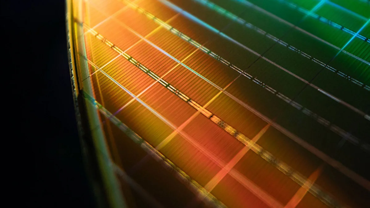
Elon Musk’s Terafab is set to receive its first EUV (extreme ultraviolet) lithography tool from ASML in mid-2027, a critical component in modern semiconductor fabrication. However, the timeline presents challenges, as the factory at Giga Texas, which is designated for chip manufacturing, won't be fully operational until late 2027. Tools will only begin to be installed then, meaning the EUV scanner will remain unused for several months, increasing the cost of an already significant investment.
The groundwork for the new fab was laid as early as April 2023, when Tesla broke ground on the north campus of its Giga Texas facility near Austin. Construction is projected to conclude by mid-2024, followed by a six-month equipment installation phase. Early production, focused on waif fabrication experimentation, is expected to start in late 2024. This careful approach is aimed at preparing the team for the large-scale production that Terafab aims to achieve with its volume fab phase 1.
Interestingly, the acquisition of an ASML Twinscan NXE EUV lithography tool reflects Terafab's initial reliance on established technology, despite Musk's previous advocacy for free electron laser (FEL) systems in semiconductor manufacturing. This choice indicates a pragmatic pivot to proven performance over experimental approaches for the startup’s first generation of machines.
Terafab plans to utilize Intel’s 14A manufacturing technology, which will require both existing Low-NA EUV scanners and newer High-NA machines. This blend aims to ensure that while the initial investments utilize traditional equipment, the potential for future technological advancements remains intact. However, introducing alternative light sources like FEL would complicate integration, necessitating extensive modifications to manufacturing processes, equipment qualifications, and quite possibly even new photomasks and photoresists.
So, while using standardized lithography equipment minimizes immediate risks, engineers at Terafab likely harbor ambitions to innovate on existing frameworks, particularly as competitive pressures grow in the semiconductor space. The landscape of chip production is rapidly evolving, and distinguishing Terafab through novel configurations may become crucial.
Recent developments show that construction at Terafab's site in Grimes County began with foundational work in September 2026. Drone footage revealed that not just land clearing, but actual structural advancements were underway, suggesting that construction is progressing efficiently. SemiAnalysis reports that the entire construction phase for Terafab's initial facility is slated to unfold over 20 months. This is quickly followed by a 17-month equipment installation schedule before ramping production to volume within six months.
Looking ahead, planned timelines indicate that Terafab could be operational by late 2029, guiding the facility towards mass production by mid-2030. A noteworthy aspect is the timing of equipment orders—SpaceX reportedly procured semiconductor manufacturing equipment as early as April 2026, prior to formal announcements surrounding the Grimes County location. This suggests strategic foresight in their manufacturing commitments in what is a highly competitive sector.
In comparison with industry giants, Intel is on track to initiate risk production using its own 14A (1.4nm-class) technology in late 2027, with high-volume manufacturing expected to commence in the latter half of 2028. This timeline reveals that Intel will significantly outpace Terafab's production capabilities, placing additional pressure on Musk’s team to accelerate processes from the very beginning.
Given this slower entry into full-scale production compared to rivals, Terafab’s offerings may not represent the cutting edge of semiconductor technology by the time they fully launch. For context, TSMC plans to bring its advanced A12 (1.2nm-class) manufacturing technology into production shortly thereafter, marking a more advanced node than what Terafab will initially utilize. Nonetheless, the specific focus of Terafab’s output—primarily serving SpaceX, Tesla, and xAI—means that slightly older technology might still meet immediate business needs effectively, especially in light of cost efficiencies derived from in-house production capabilities.
The road ahead for Terafab involves navigating both technological and logistical hurdles as it carves out its niche in semiconductor manufacturing. With the right execution strategies, despite potential setbacks in technology sweet spots, this endeavor stands to serve Musk’s larger technological ambitions in a rapidly developing industry.
As Musk's team moves forward, keeping an eye on their pace relative to industry innovations and efficiency will be essential. These dynamics could shape not only their competitive edge but also the broader context of chip production as the demands of modern technology evolve.